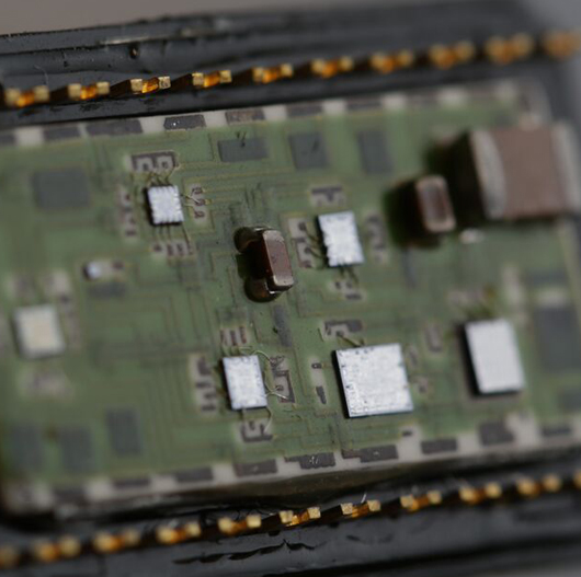
Thick Film Technology is at the heart of our microcircuit technology and is superior to both PCBs and conventional MCBs. The background substrate is typically ceramic, titanium and stainless steel. This is screened with conductor, insulator and resistor material to form the circuitry. The technology used to lay down the circuitry results in a much thicker and consistent layer than in acid etched conventional microprocessors. This is the key to their enhanced performance and reliability.
The advantageous properties of materials like ceramics allows our circuit boards to be used in the harshest environmental conditions, including extreme high and low temperatures, thermal shock applications, high humidity, high vibrations, and under extreme acceleration/deceleration. Our Thick Film Microcircuits are generally smaller and more secure than both PCBs and traditional MCBs.
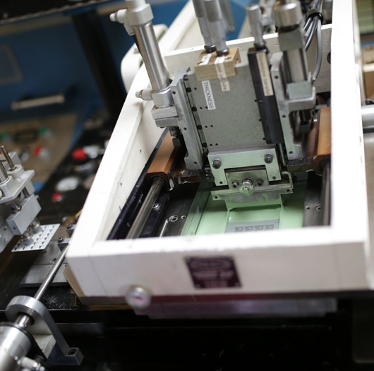
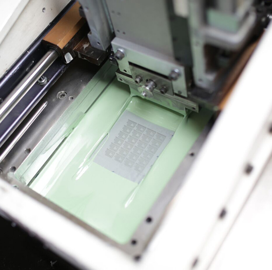
Thick Film Microcircuits are made using a combination of specialised micro screen printing and firing of layers of conductor, resistor and insulator inks on a substrate. The process begins with a schematic diagram being transferred to a set of screens for printing and firing.
Like pottery, the printing and firing is done in layers - each individual screen print is fired in an oven with the total number of prints dependent on the complexity of the circuit. A laser beam then cuts a track in the fired resistor ink, setting the precise value and tolerance of resistors. The surface mounted components, if required, are then attached and the final circuit is washed, inspected, encapsulated, labeled and every unit quality tested prior to leaving our facility.

Thick Film Microcircuits offer a highly reliable solution for many purposes such as medical, space, defence, automotive, electronic entertainment devices, R&D, info and communication systems, high-frequency applications and high-power/high-voltage electronics.
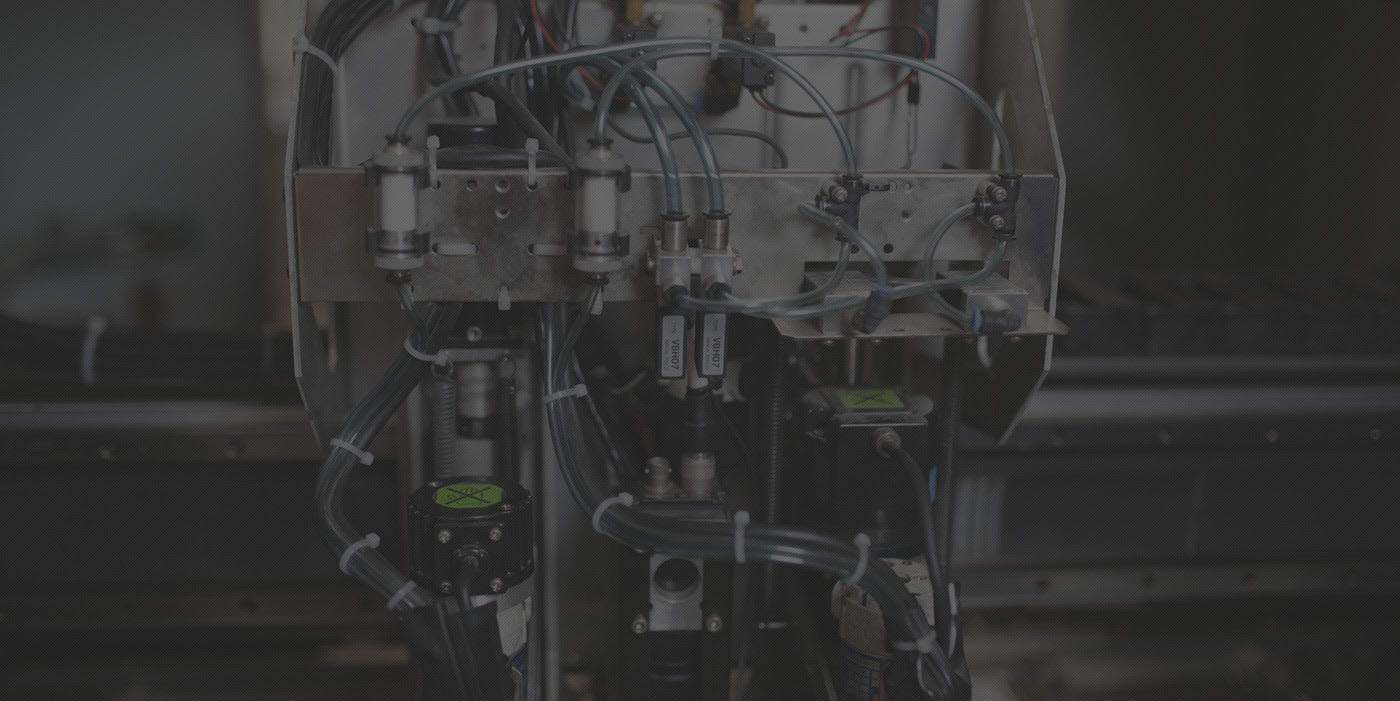
Whether you need assistance with new product development and prototype parts, or full production runs of manufactured product, we have the experience and capabilities to support your Thick Film needs.